The EMINENT project is concerned with the following research areas: (i) emerging memory technologies (memristors and spintronic devices) used in a non-Von Neumann context, (ii) hardware implementations of bio-inspired neural networks (Spiking Neural Networks), (iii) hardware dependability (robustness, reliability and test) and design-for-dependability. The goal of the EMINENT project is to provide a dependable Emerging Memory-based Spiking Neural Network architecture. This goal will be achieved by fulfilling the following objectives: (i) study of meaningful dependability threats in SNN architectures, (ii) reliability estimation campaign; (iii) manufacturing test strategy and design-for-test solutions; (iv) strategy for architecture dependability improvement.
The research hypothesis of the EMINENT project: the strong restrictions on the size of embedded Spiking Neural Network architectures (limited silicon area and interconnectivity ability) require minimization of the network redundancy which in turn reduces its the intrinsic fault tolerance. Therefore, there is an acute need to evaluate the reliability and perform manufacturing test of the neuromorphic hardware architectures to guarantee their correct operation and robustness.
Context
The EMINENT project is concerned with the following research areas:
- emerging memory technologies (memristors and spintronic devices) used in a non-Von Neumann context,
- hardware implementations of bio-inspired neural networks (Spiking Neural Networks),
- hardware dependability (robustness, reliability and test) and design-for-dependability.
The emerging memory technologies favor increasing system complexity and performance, opening the scientific community to great improvements in state-of-the-art computing (such as high performance computing or approximate computing) but also to new applications and computation paradigms (such as in-memory computing or neuromorphic computing) which had been unfeasible a few years back due to technological limitations. This project mainly focusses on the use of memristors or spintronic devices as artificial synapses for bio-inspired computing architectures. In this context, they have double functionality: memory (to save the values of the synaptic weights) and computation (to facilitate the on-line learning process, i.e., update synaptic weights).
The Spiking Neural Networks (SNN) are widely studied nowadays due to the high level of realism they bring to neural simulation, their energy efficiency and their ability for on-line learning. The related bio-inspired learning rule is known as STDP (Spike Based Dependent Plasticity) and is applied on each synapse independently of the global state of the network. In return, the synapse must be doted of computation capabilities. A hardware implementation of an SNN requites architectural co-localization of the processing and memory (non-Von Neumann architecture). The circuits solutions used to implement silicon neurons are application depended, but the vast majority are built with a temporal integration block, a spike generation block, a refractory period mechanism, and a spike adaptation block. Synapses are required to exhibit plasticity (i.e., modulation in their efficacy) and to support online learning algorithms, that manifest in changes in their strengths. Emerging memory devices can be used as synaptic elements thanks to their tunable conductivity, compatibility with advanced CMOS fabrication process, low power consumption, non-volatility and scalability. The synaptic conductance modulation can be emulated using:
- the analog approach (cumulative decrease and increase of resistance), where multiple resistance states emulate long-term potentiation and depression;
- the binary approach, uses two distinct resistance states per device associated with a probabilistic programming scheme.
Hardware dependability describes the ability of a system or component to function under stated conditions for a specified period of time. Dependability issues in hardware come from the manufacturing process, or operation and environmental conditions. Manufacturing induced variability, defects, stochastic effects, and aging degradation can cause important variations of the electrical characteristics of fabricated devices which in turn can lead to device failure. Manufacturing test together with design-for-reliability solutions assure the quality and reliability of integrated circuits.
Objectives
The EMINENT project focuses on a fully-connected SNN, that learns using the Spike Timing Dependent Plasticity (STDP) method with lateral inhibition, with integrate-and-fire neuron and resistive synapses. Both analog and binary approach for synaptic conductance modulation will be used. In order to achieve the project’s goal (robust and efficient hardware implementation of SNNs) one has to jointly-consider the characteristics of the SNN itself (connectivity, neuronal activation function, learning rule and synaptic update), the characteristic of the devices used to implement it (CMOS ON/OFF current and threshold voltage, conductivity modulation and current-compliance of the synaptic devices, etc.) and the environment in which the circuit will be deployed.
Objective 1:
The dependability study will be performed by two approaches: top-down and bottom-up. In the top-down approach the correctness of the SNN algorithm is evaluated under neural and synaptic death, the results will be validated by system level simulation of the SNN architecture. In the bottom-up approach we will evaluate the effect of fabrication-induced defects and variability on the operation of the neuron and synapse and a fault modeling campaign will be conducted. These faults will be injected at system level and the robustness of the SNN will be evaluated. Based on these analyses we will be able to provide metrics to qualify a good/degraded but still functional/failed neural network.
Objective 2
The reliability estimation campaign will be conducted in a bottom-up approach. At gate level, we will evaluate the effect of aging phenomena, noise injection, and severe operation and environmental conditions. This analysis will culminate in a fault modeling campaign. These faults will be injected at system level, and the robustness, failure rate and mean time to failure (MTTF) of the SNN will be evaluated.
Objective 3
A comprehensive post-fabrication test campaign will be conducted. Both functional and structural test strategies are targeted. We will follow the conventional approach used today to test integrated circuits (using test input vectors able to target all possible faults). SNN architectures resort to the combination of devices with both deterministic and stochastic behaviors and they include both digital and analog elements. A test strategy suitable for SNNs should be able to test the correct operation of both neurons and synapses, it should be economical (in area, power and performance overhead), it should not depend on the training data nor on the context the network would be used. To devise efficient testing strategies will get our inspiration from techniques like March Tests, Iddq (measuring the supply current in the quiescent state), Analog-to-Digital Converter (ADC) testing, true random number generator (TRNG) testing. In parallel we will design test access mechanisms which ideally will allow for (i) independent testing of the synaptic array and neuron layer for structural integrity, and (ii) jointly testing the SNN for functional correctness. Moreover, design-for-test (DfT) and built-in-self-test (BIST) techniques will be devised.
Objective 4
We will provide solutions for architecture dependability improvement which can be based on robust circuit design, defect-aware design, hardware redundancy, design diversity, dynamic reconfiguration, dynamic adaptive signal control, etc.
Dissemination
DATE 2020 Friday Worksop - Computation-In-Memory (CIM): from Device to Applications
- Device and technology: physics and modeling, device technologies, device characterization.
- Novel logic and circuit design concepts using NV devices: Boolean logic, threshold logic, arithmetic circuits, multi-level based logic, memories, PUF technology, TRNG design.
- System architectures and new computing paradigms: resistive computing, neuro-inspired computing, novel architectures and CMOS integration, cellular automata and array computing.
- Applications exploiting NV devices: signal processing, chaos and complex networks, sensors applications, AI applications.
- Automation and CAD tools: mapping tools, compilers, logic synthesis tools, design space exploration tools.
- Test and Reliability: test and reliability solutions for circuits and architectures.
|
TIMA Scientific Days - AMS-RF circuits and systems
07 April 2020, Grenoble, France
14h-14h30 Elena-Ioana VATAJELU – Design Considerations for Spiking Neural Networks
|
ETS 2020 Fringe Workshop - AI-TREATS: 1st workshop on AI Hardware: Test, Reliability and Security
- Testing: fault modelling, fault simulation, test generation, post-manufacturing testing, design-for-test, built-in self-test, on-line testing.
- Reliability: reliability analysis, design-for-reliability, fault-tolerance, self-repair, functional safety.
- Hardware security and trust: IP/IC piracy, hardware Trojans, side-channel attacks, fault injection attacks.
|
Project Results
Basic Setup:
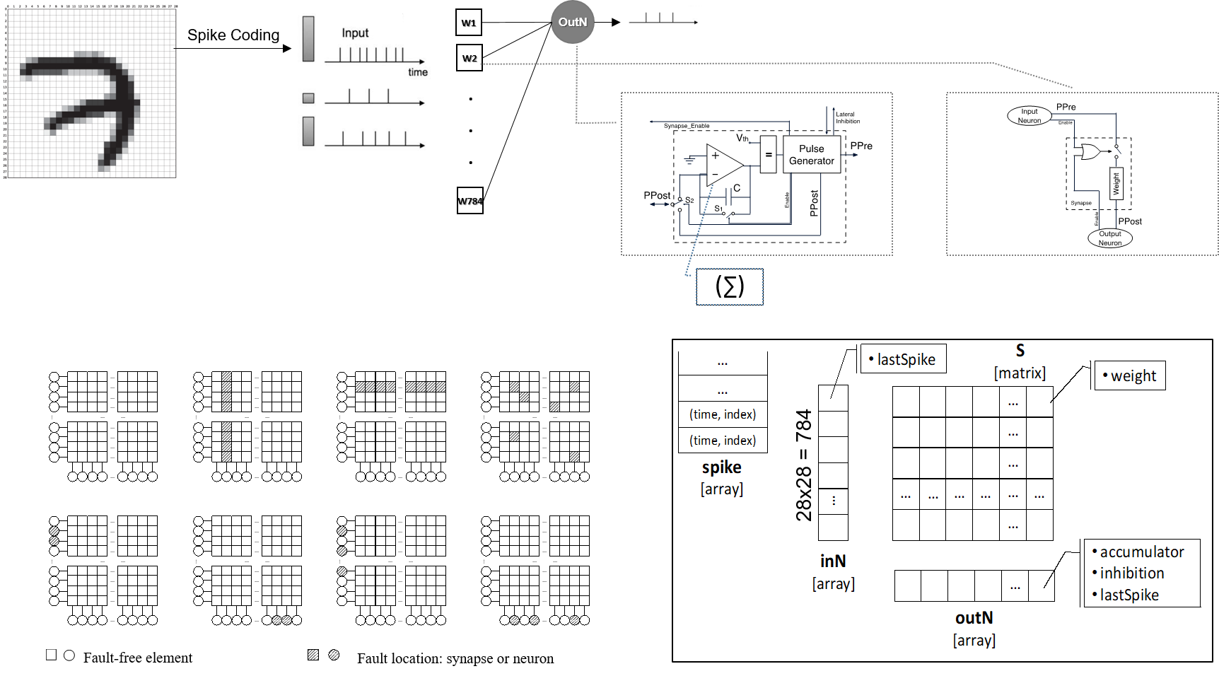
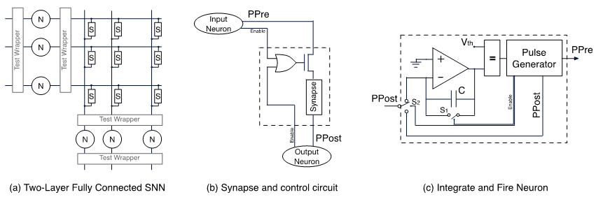
The EMINENT project focuses on a fully-connected SNN, that learns using the Spike Timing Dependent Plasticity (STDP) method with lateral inhibition, with integrate-and-fire neuron and resistive synapses (see Fig. 1). Both analog and binary approach for synaptic conductance modulation will be used. Fig. 1a) sketches the connectivity between two consecutive layers of such a network. Here N represents a spiking neuron, S represents a synapse and test wrapper is the circuitry not-pertaining to the SNN but necessary to perform the manufacturing test, to be designed in the EMINENT project framework. The synapse and its control circuit are illustrated in Fig. 1b). Several works propose using the resistive-based synaptic devices in a crossbar array (without access device) to assure minimum area footprint. However, such implementation suffers from large leakage currents in the half accessed cells (gravely detrimental to the learning process) and from inefficient forming process (when RRAM devices are used for synapse) and un-controlled current compliance (can cause synapse deterioration or inefficiency). For this reason, in the presented design, an access transistor is used for the access to each synapse. This transistor should isolate the synapse from the rest of the network when there is no activity on either of its connected neurons, and it should allow the passage signal coming from either of the neurons. This behavior is guaranteed by OR-ing enable signals generated by the neurons.
Fault Injector Setup: